Modular Test System Part 1

This is the first post about a modular test equipment / data acquisition system I'm working on. I had the opportunity to work with PXI based equipment on several projects back when I was in school. I really liked these systems because they made it easy to plug in a card for any type of I/O and get data in or out of PC software easily. It is possible to do things like capture samples with an oscilloscope card, process them in software, then drive a signal generator output based on the result. Something that would be much more difficult with individual pieces of equipment. The problem with PXI gear is the cost. It is generally far too expensive for home use.

So I decided to build my own. Not something as capable as PXI, but a simpler and lower cost version which will be enough for my uses. The overall architecture includes a main controller, up to 8 I/O cards, and backplane to connect them all. The main controller handles data processing and interfacing with a PC, while interfacing to each I/O card through an SPI interface. The backplane distributes power, SPI, and a few other signals between cards. I/O cards interface between SPI on the backplane and, well, pretty much anything. I have built a few low speed analog and digital output cards to start. Once the basic platform is working I have a list of other ones to design.

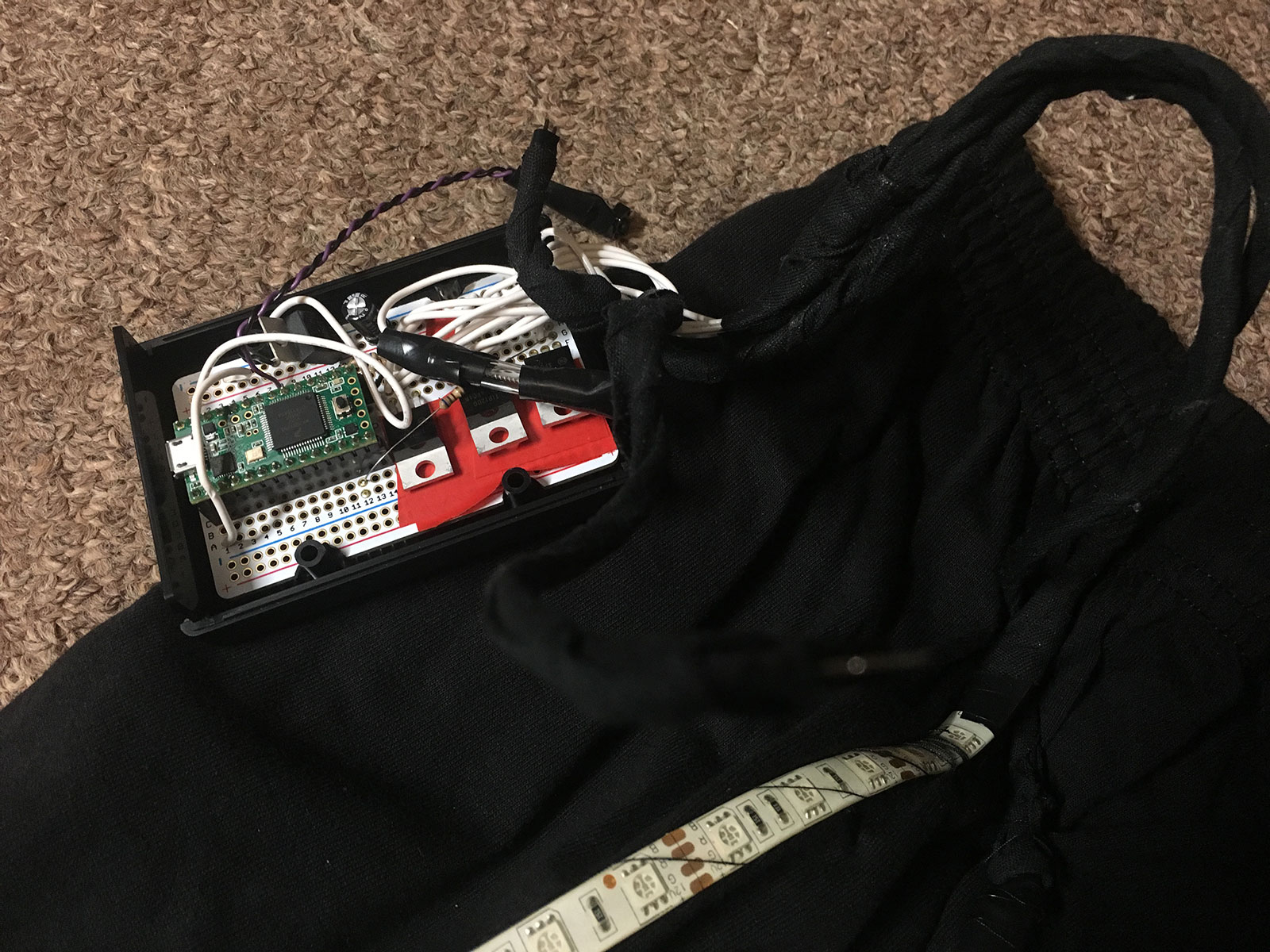
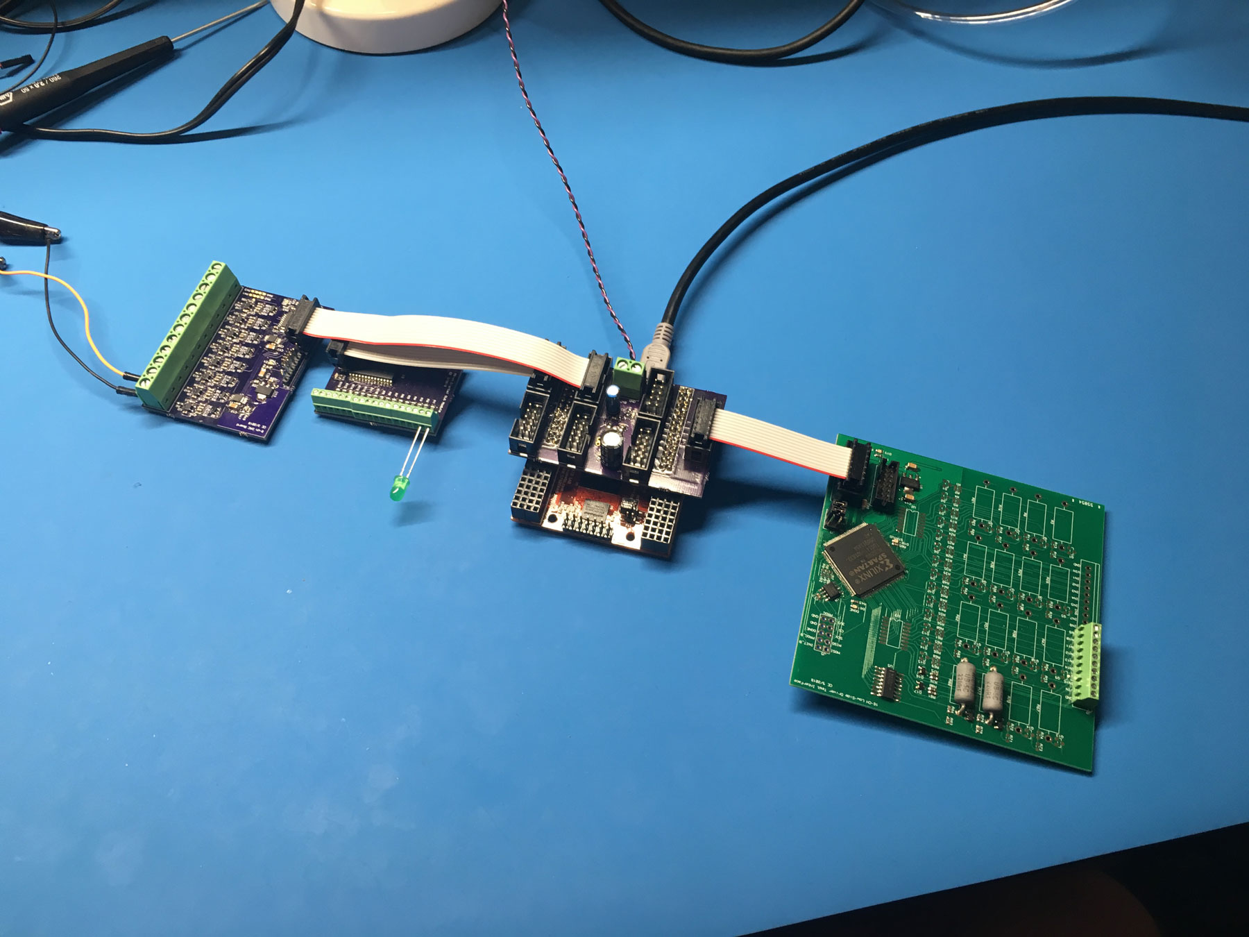
The first iteration of this project last year was just a breakout board on top of a Numato Saturn FPGA dev board with 10-pin ribbon cables to connect each card. Made for a cheap way to test things out without building a full controller and backplane. From left to right in the photo below:

  • Analog output card - 8 channels of 0-30V outputs at up to 10kHz
  • Digital I/O card - 16 channels of 5V digital I/O
  • Controller - Saturn FPGA board on bottom, breakout PCB on top
  • PWM input card - 16 inputs designed to interface with low-side drivers. Switchable 5W load resistor on each channel. Inputs go to an FPGA to allow frequency and duty cycle measurements.

First prototype system

After that, I started planning the card design. Two decisions were made to keep cost down: The card size is 3.9" square, which just fits inside the 10cm max size where cheap boards can be ordered from many PCB fabs. Also, standard PCIe connectors are used. The connector housings are super cheap due to being made in large quantities for PCs and the mating half is free (PCB contacts). While they are still able to support high speed signals with proper layout. The only downside of this design is the card dimensions don't fit any existing standard, which makes finding a chassis harder. I ended up using a Vector CCK12S-H/90, which is a small rack kit with adjustable rails to handle various card sizes. This ends up not being a great solution, but I will get into that with the next blog post.

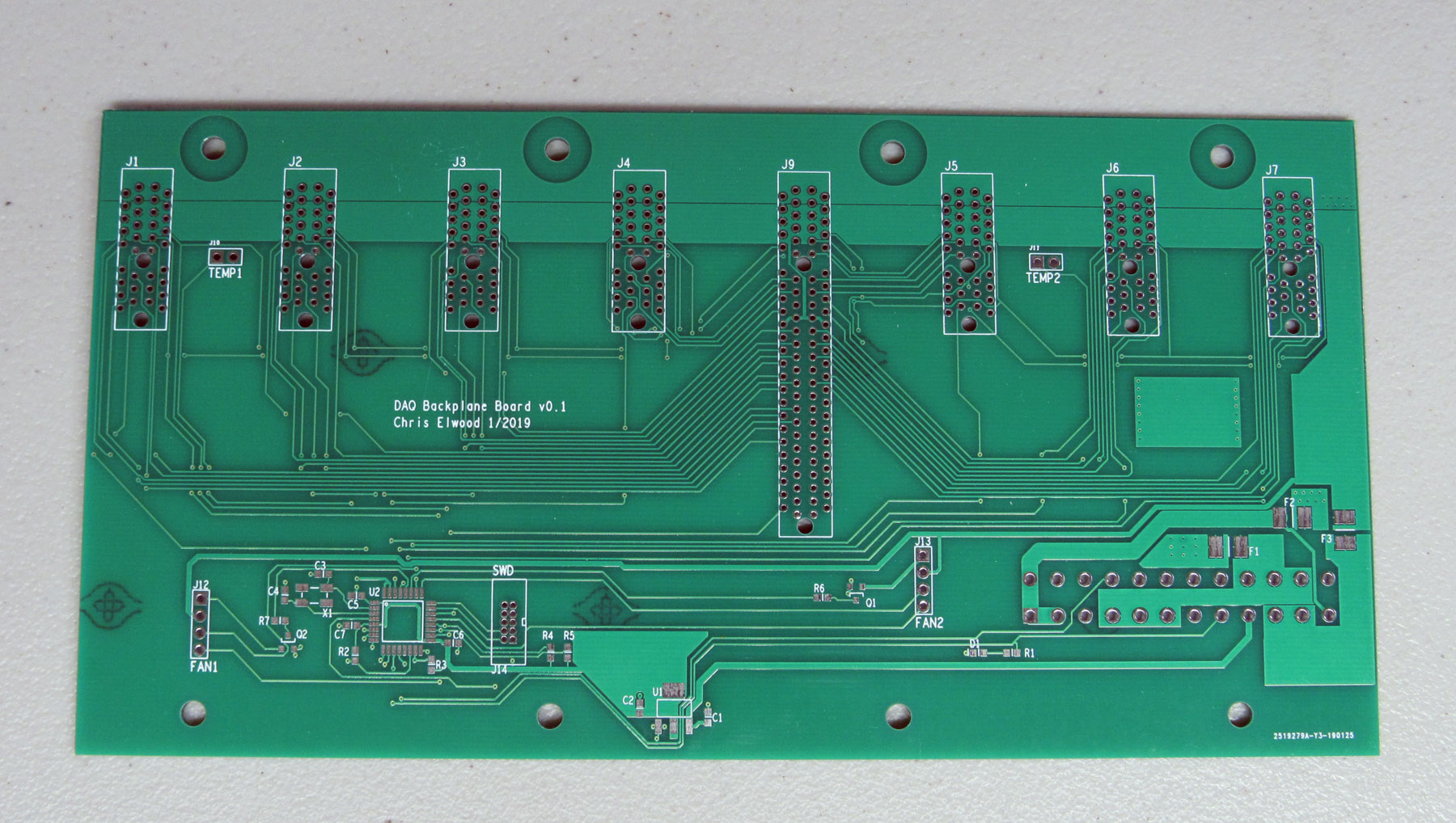
With the form factor decided, I started on a backplane PCB. This first one supports a controller and 7 cards (controller can handle 8, but the chassis is only wide enough to fit 7). It provides an independent SPI bus from the controller to each card, a common I2C bus (for identifying cards), and power (supplied from an ATX power supply connected on the back). There is also a STM32 microcontroller to monitor temperatures and drive fans if needed.

Backplane PCB

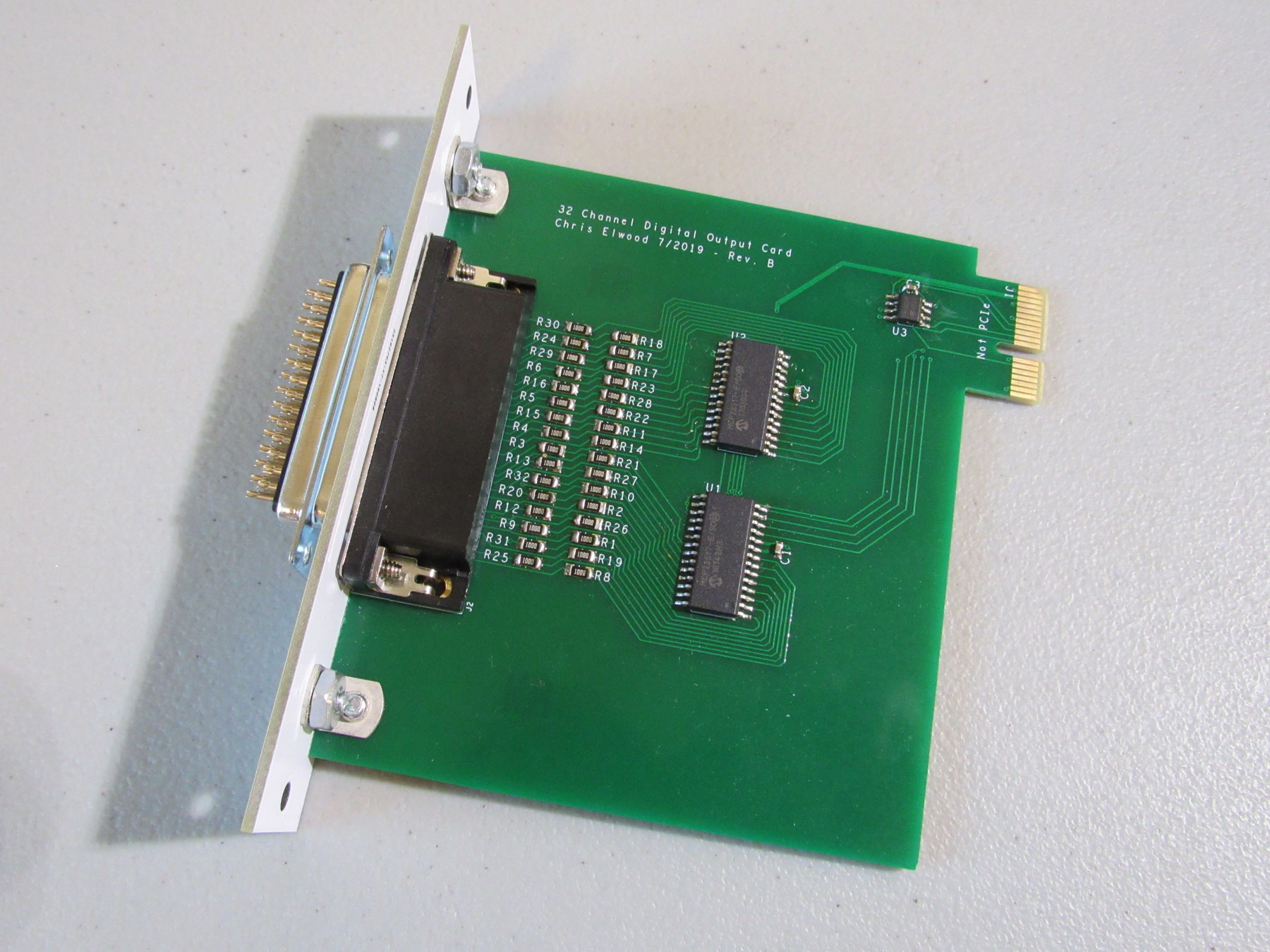
The next step was creating the first I/O card. I started with a digital I/O card because it was the simplest and I needed to work out the mechanical design. The front panel is a white PCB, attached with two angle brackets. On the first version, I put the angle brackets too close to the edges of the main PCB and they hit the card guides in the chassis, preventing the card from being inserted. The second version, shown below, fixed this and made some other minor improvements. Electronics wise, it is simply a pair of MCP23S17 GPIO expanders.

Digital I/O card

With that done, it was time to build a proper controller. I decided to go with a FPGA + microcontroller architecture. The FPGA handles the 8 SPI interfaces to the I/O cards and can offload any timing critical operations from the micro. The micro runs application code and provides USB and ethernet interfaces to a PC. I am using a Xilinx Spartan 7 FPGA and STM32H7 micro. The FPGA is connected to the external memory interface of the STM32 as if it were an SRAM. This allows registers to be created in the FPGA design and mapped into the STM32 memory space as if they were peripherals on the micro itself. There is a 100Mbit ethernet PHY for networking and a FT232H chip for high speed USB. An SD card slot is also included as another option for storing data.

Controller board

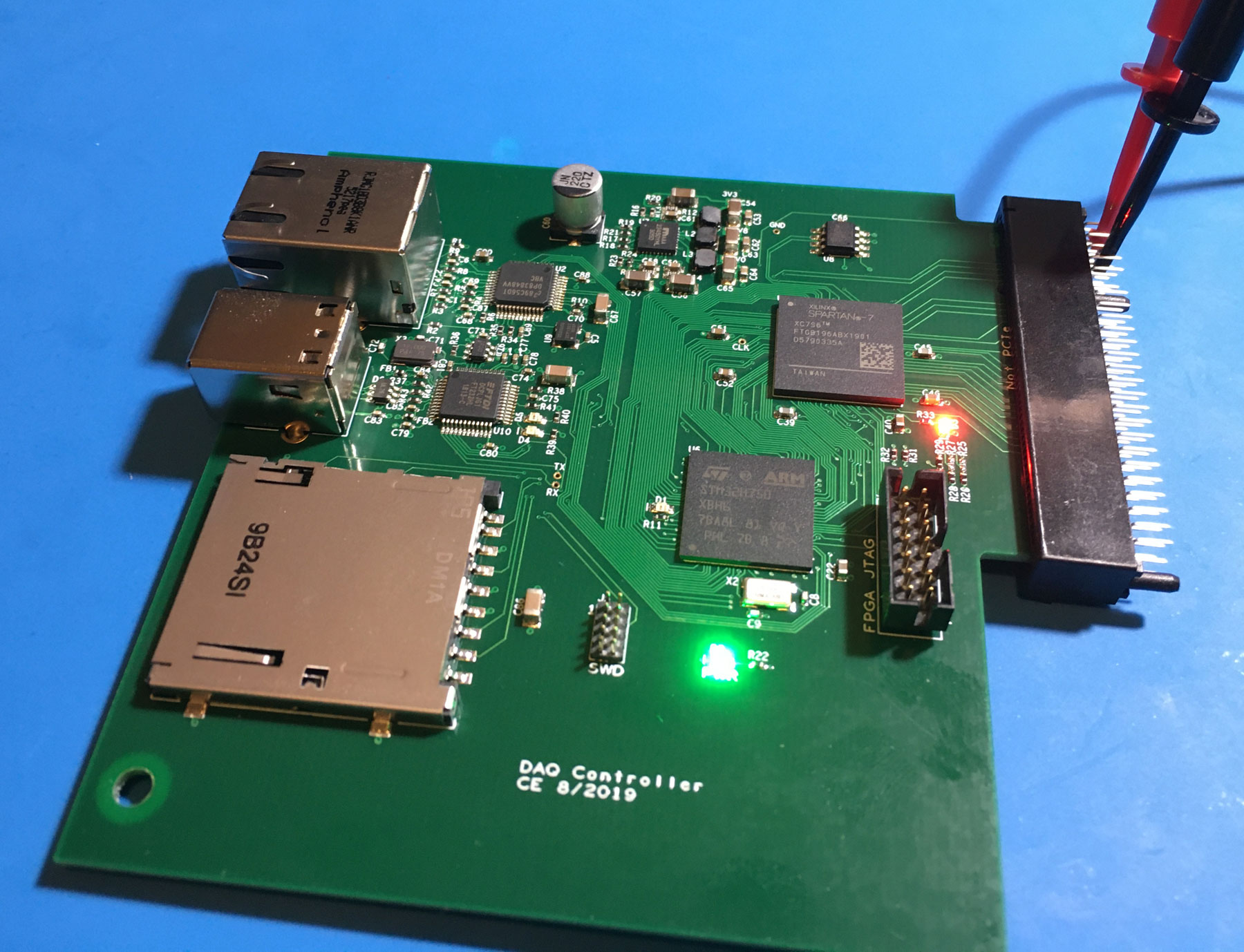
This board was my first attempt at using large BGA packages. The FPGA is a 196 ball, 1.0mm pitch package. The STM32 is 265 balls, 0.8mm pitch. I was a little worried about soldering them, but it actually didn't turn out to be a problem at all. I followed the manufacturer recommended PCB pads for each and included a full silkscreen outline for aligning the chips during placement. This worked well. For the ethernet PHY and USB chip I chose QFP instead of QFN packages because I was worried about soldering the QFNs. Having more experience now, I wish I had done it the other way. I've had more issues with solder bridges on QFP chips due to the long and closely spaced pins, while QFN chips have been easier than expected to work with. I may actually replace the ethernet PHY entirely on the next revision. This board uses a DP83848, which has a bunch of annoying quirks. I have since found some alternatives which are both better and cheaper

I learned a couple lessons on layout with this board too. I usually place parts, route signal nets, then do power planes last. In this case I placed the FPGA and STM32 where you see them in the photo above and routed all the signals to each. I was going to put the power supply near the botttom of the board (in what is now empty space). I ran into an issue when I looked at the FPGA though. It has three power rails: 3.3V IO, 1.8V AUX, and 1.0V core. The CPGA196 package it's in is designed for 4-layer boards and has its power connections arranged to be easily routed on one plane layer:

FPGA power plane layout

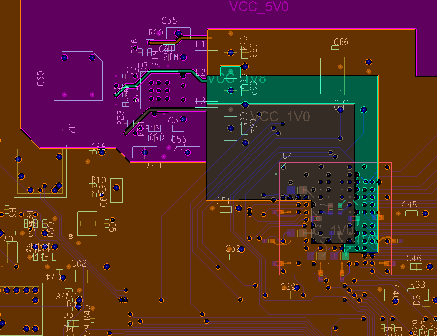
The FPGA is U4, outlined in red on the right. The 3.3V IO voltage (orange) connects to balls around the outside. The 1.0V core voltage (gray) connects in the center. The 1.8V aux voltage (green) is to the right of the core voltage connections. There is an area with no IO power connections at the top, which gives space to get the aux and core power planes out on the same layer. Problem is, it forces you to break them out in that direction. And I couldn't easily rotate the FPGA due to the already routed signal connections. If I wanted to keep the power supply at the bottom of the PCB, those planes would have to come out the top, turn around 180 degrees, then pass under the STM32 to get to the power supply. This would break up the main 3.3V plane (4 layer board, so I only have a single layer for power) and cause other problems. So I ended up having to move things around and cram the power supply in at the top. Something that could have been avoided if I looked at the power layout earlier in the process.

So far I have some minimal software written. The FPGA has a state machine to initialize the digital I/O card over SPI and update its outputs based on commands from the STM32. The STM32 has enough code to bring up the hardware and pass through commands sent from a PC over USB. I have a python script on the PC which currently just blinks an LED on the I/O card.

There is much more I want to do in this area. Each I/O card will need a driver with three parts: FPGA module, embedded driver code, and PC code. I need to define standard formats for each of these so drivers can be loaded in based on the cards present in the chassis. Ideally, the software will identify each card based on its I2C EEPROM and configure itself appropriately. A lot of work is needed to get to that point though.

One downside of this architecture is that the signals for each card slot connect directly to FPGA pins. So changes in card configuration will require recompiling the FPGA bitstream. Meaning the user will need the whole Xilinx toolchain installed. Not ideal, but I don't see a way to avoid it without majorly reducing flexibility or making the cards more complicated. I have used commercial systems which behave the same way (require FPGA rebuild when cards are changed), so it is not completely without precedent.

Full test system chassis

There are some design choices I am questioning now that the whole system is together. It was originally intended for a specific project and had some compromises which made sense for that project. But I'm now leaning towards it being a more general purpose platform. I'll get into this more in the next blog post, where I cover the second revision hardware I am currently working on.

Design files and draft mechanical and electrical specification documents are on my github. Be aware these are very much a work in progress and will likely change.

Project Log

I recently put together descriptions of all my in-progress projects, which can be found here. This page can also be accessed from the "Projects" button in the navigation bar above.

I tend to have multiple projects going and switch between them depending on what I'm interested at any given time. This means it can take a while for a project to reach the point where I can write a full blog post about it. I wanted to provide some view into what I'm working on that hasn't reached this page yet. As projects are completed, I will move them from the projects page into more detailed blog posts. I will leave links on the projects page though, so it can act as an index for the site.

STM32 / FPGA Board

I put together a development board of sorts last month to test out a few different things. It consists of a STM32F4 microcontroller with its external memory interface connected to a Xilinx Spartan-6 FPGA. The FPGA has a basic VGA output as well as SDRAM to use as a frame buffer. An ethernet PHY is also attached to the microcontroller. This project serves several purposes:

  • More complex project to continue learning how to use OrCAD.
  • Test bed for an architecture I'd like to use in the future where the STM32 FSMC is used to interface to an FPGA and map "registers" created in the FPGA into microcontroller memory space.
  • Test board for DP83848 ethernet interface circuitry.
  • Not originally planned, but my first try at assembly using solder paste and reflow.

This board isn't super complicated electrically, but took a while to design because I had to create new components and footprints for most of the parts. I have a decent parts library now, so this was a good use of time though.

The challenging part for this project was assembly. I was planning to hand solder it, but the timing lined up with when I started researching reflow soldering for another project. So I decided to order a stencil and use solder paste plus a toaster oven instead. Unfortunately, I didn't get a decent photo of the board before it was fully assembled, but there is a short video clip here of the reflow process. There were a couple mistakes I made in the process. Two components (SDRAM and SPI flash) did not have stencil openings because I forgot to define paste mask openings when creating the pads for those packages. A ton of the pins on the STM32 and FPGA also ended up bridged after reflow... likely due to me not holding the stencil down well enough and getting too much paste applied. Soldering the messed up parts by hand plus using lots of solder braid to clear the bridged pins resulted in the final result shown below.

Assembled board, after a lot of hand rework.

After cleaning up all the soldering issues and getting to the point where the 3.3V rail and ground weren't shorted, I powered the board up. Fortunately, board bring-up went better than the soldering did. I was able to connect to the STM32 and the FPGA with their respective programming interfaces and verify that both were functional.

The only fail electrically was the clock source for the DP83848 ethernet PHY. The PHY requires its own 25 or 50 MHz clock source because the frequency is not a multiple of the 12 MHz crystal used for the micro. I placed a 25 MHz crystal to cover this. When reviewing the PHY datasheet before ordering parts, I discovered that in RMII mode (which I'm using) it needs a 50 MHz oscillator. A plain old crystal can only be used for 25 MHz clock when in full MII mode. I caught this and ordered a 50 MHz oscillator that fit the same footprint as the crystal I had designed the board for. Thought this solved the problem... kinda forgot that oscillators need power and ground though, which are not routed to it since I was going to use a crystal. Oh well, I'll have to bodge the oscillator in with some jumper wires before I can test ethernet.

Software wise, at this point I have some basic test code running on the STM32 and text output on VGA working. I had a mostly working verilog design for VGA output from another project, so that didn't take long. It is purely text-based, using characters from a text buffer in block RAM to index into a "font ROM" which defines the pixels to display for each character. All that had to be added was a serial interface for writing to the text buffer RAM, so the STM32 could control what was displayed.

VGA output testing.

Next step from here is to build a controller to use the SDRAM chip on board. This is needed to have a full resolution frame buffer, as block ram in the FPGA is much too small to hold a full video frame. Until then, only text can be displayed. I have read a few articles and have a pretty good idea how this will work, but it is still a significant amount of verilog to write. After that, I need to get the FSMC (external memory interface) in the STM32 set up. Communication between the STM32 and FPGA is currently only a slow serial port. Ethernet needs to be tested too. I have working code for this from another project, so it should be easy once the oscillator is fixed.

LED Matrix Clock

It's been a while since I've updated this site. There was too much going on with school at the time and I just didn't end up getting time to write projects up. I graduated a while ago now and have more free time, so I'm going to make an effort to post here again. Starting off with a small project:

I have been moving my PCB design work over to OrCAD this year and needed a simple test project to learn the workflow in the new software. Adafruit has some neat looking LED matrix modules that I wanted to use somehow. This was the result:

Finished clock.

The above photo was taken before I implemented brightness control. It is dimmed to be a bit less blinding now. The electronics are pretty simple. A STM32F0 microcontroller controls everything. Three 74HC595 shift registers drive the columns and a ULN2003 transistor array is used to switch the rows. The LEDs all run directly off 5V input power and the micro is supplied by a 3.3V regulator.

PCB side of the clock.

I made the mistake of designing around a ULN2803 (8 channels vs 7 on the ULN2003) without realizing that they come in a wide SOIC package. Ended up using a ULN2003 plus a SOT23 FET for the 8th channel to make it work. In addition, I tied the BOOT0 pin on the micro to VCC instead of GND, which forced it into bootloader mode instead of running my code. A lifted pin and another jumper wire fixed that.

Halloween Costume

It's been a couple weeks since halloween, but this is worth writing up anyway. Last year I had been thinking about doing some sort of costume using LEDs. The prices on flexible RGB LED strips have gotten really cheap, so it seemed like a good time to try to build something with them. I hadn't come up with any good ideas for what to actually make until a few days before Halloween, when a friend showed me a video of an LED stick figure costume that had gotten a lot of attention last year. So, a few days before Halloween, I decided to try building my own. Thanks to the magic of Amazon, I got a 5 meter roll of LED strip shipped next day for $15. An old sweatshirt and pants were found to attach everything to.

Putting it together was fairly simple: lay out each section of strip and cut it to length, solder wires on, then stick it in place using the adhesive back on the strip. Each section was wired in parallel so they would all light up the same color. The power supply and controller are directly connected to the section on the pants, which the sweatshirt then connects into with a 4-pin header.

Terrible mirror photo of the costume.

I only had a couple hours to throw the controller together and get everything working, so I stuck to using a Teensy 3.1 for simplicity. TIP120 transistors are used to control each of the red, green, and blue channels. The whole thing is powered from a 3S RC battery via a 5V voltage regulator. The LED strips can draw over an amp when all three colors are on full brightness, so the regulator really should have had a heat sink. As it turned out though, running the LEDs at a max of about 20% PWM duty cycle was more than bright enough at night. With the patterns I was using, power usage was only in the 100-200 mA range, so everything could run off of a tiny 1000 mAh battery for several hours.

Controller built on protoboard in its enclosure.

Since the Teensy is programmed the same as an Arduino, getting the code working was easy. At first, I just made a simple pattern that fades in random colors. I later added a button to switch between modes and made a few more patterns. One of those was strobe mode, which flashed white at full brightness… it produced quite the effect outside in the dark!

It all ended up working well for something thrown together last minute. The adhesive on the LED strips held onto fabric better than expected, although not enough to be a permanent solution. After the first night running around with it, some of the strips were peeling off, so I spent much of the next day sewing everything on permanently. Very tedious (probably since I have no idea how to do it correctly), but made things much more durable.

Page 1 / 2 »